- 您现在的位置:买卖IC网 > Sheet目录1990 > BU3076HFV-TR (Rohm Semiconductor)IC CLOCK GEN 1CH HVSOF6
Technical Note
2/21
www.rohm.com
2009.04 - Rev.A
2009 ROHM Co., Ltd. All rights reserved.
BU3071HFV,BU3072HFV,BU3073HFV,BU3076HFV,BU7322HFV,BU7325HFV
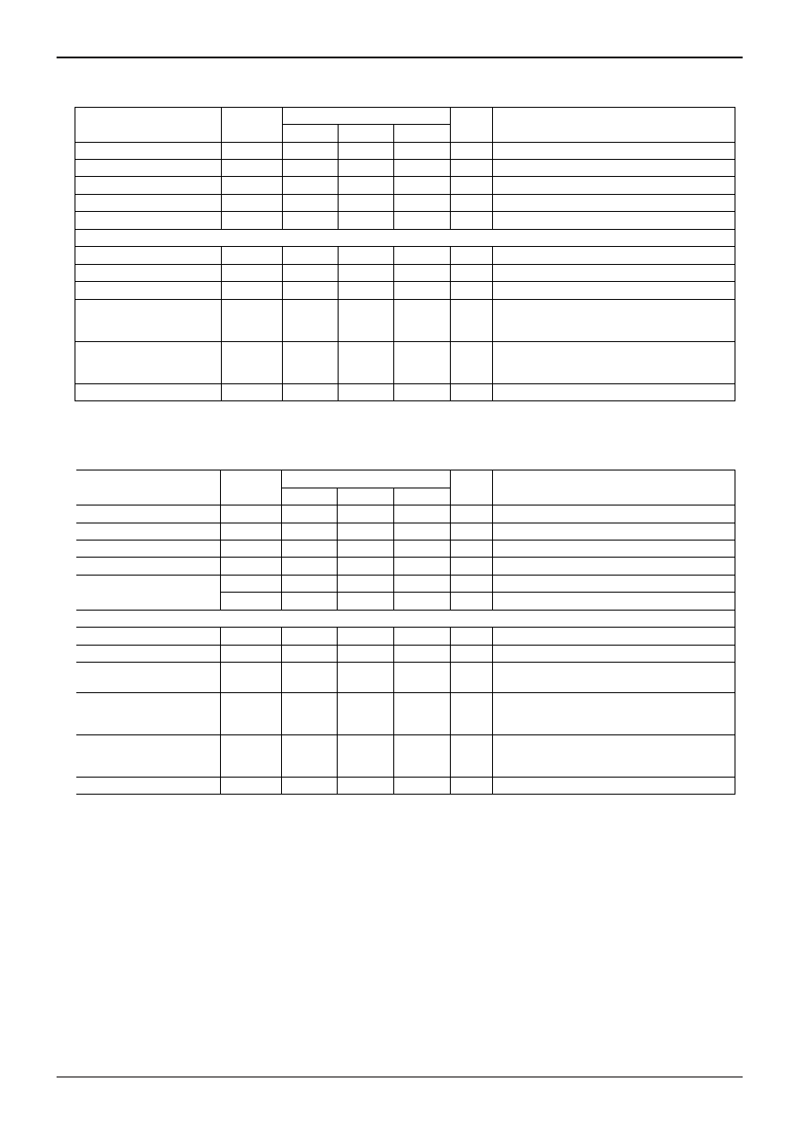
●Electrical Characteristics
BU3071HFV(Ta=25℃, VDD=3.3V,Crystal frequency=28.6363MHz, unless otherwise specified.)
Parameter
Symbol
Limits
Unit
Conditions
Min.
Typ.
Max.
Output H voltage
VOH
2.8
-
V
IOH=-4.0mA
Output L voltage
VOL
-
0.5
V
IOL=4.0mA
Consumption current 1
IDD1
-
10
15
mA
OE=H, at no load
Consumption current 2
IDD2
-
1
1.3
mA
OE=L
Output frequency
-
54.0000
-
MHz
IN*264/35/4
The following parameters represent design guaranteed performance.
Duty
45
50
55
%
Measured at a voltage of 1/2 of VDD
Period-Jitter 1
σ
PJsSD
-
50
-
psec
※1
Period-Jitter MIN-MAX
PJsABS
-
300
-
psec
※2
Rise time
tr
-
2.5
-
nsec
Period of transition time required for the
output to reach 80% from 20% of VDD.
Provided with 15pF output load.
Fall time
tf
-
2.5
-
nsec
Period of transition time required for the
output to reach 20% from 80% of VDD.
Provided with 15pF output load.
Output Lock time
tLOCK
-
1
msec
※3
Note) The output frequency is determined by the arithmetic (frequency division) expression of a frequency input to IN.
If the input frequency is set to 28.6363MHz, the output frequency will be as listed above.
BU3072HFV(Ta=25℃, VDD=3.3V, Crystal frequency=48.0000MHz, unless otherwise specified.)
Parameter
Symbol
Limits
Unit
Conditions
Min.
Typ.
Max.
Output H voltage
VOH
2.8
-
V
IOH=-4.0mA
Output L voltage
VOL
-
0.5
V
IOL=4.0mA
Consumption current 1
IDD1
-
11
16
mA
PD=H, at no load
Consumption current 2
IDD2
-
5
A
PD=L
Output frequency
CLK_27
-
27.0000
-
MHz
SEL=L, IN*18/8/4
CLK_36
-
36.0000
-
MHz
SEL=H, IN*24/8/4
The following parameters represent design guaranteed performance.
Duty
45
50
55
%
Measured at a voltage of 1/2 of VDD
Period-Jitter 1
σ
PJsSD
-
35
-
psec
※1
Long-Term-Jitter
MIN-MAX
LTJsABS
-
0.9
1.5
nsec
MIN-MAX of long-term jitter
(100 sec from trigger)
Rise time
tr
-
2.5
-
nsec
Period of transition time required for the
output to reach 80% from 20% of VDD.
Provided with 15pF output load.
Fall time
tf
-
2.5
-
nsec
Period of transition time required for the
output to reach 20% from 80% of VDD.
Provided with 15pF output load.
Output Lock time
tLOCK
-
1
msec
※3
Note) The output frequency is determined by the arithmetic (frequency division) expression of a frequency input to IN.
If the input frequency is set to 48.0000MHz, the output frequency will be as listed above.
发布紧急采购,3分钟左右您将得到回复。
相关PDF资料
CA3338AMZ96
IC DAC 8BIT 50MSPS R-R 16-SOIC
CDCR83DBQG4
IC DIRECT RAMBUS CLK GEN 24-QSOP
CDP68HC68T1M
IC RTC 32X8 NVSRAM CMOS 20-SOIC
CPLL66-1600-2200
IC VCO PLL/SYNTH 2.2GHZ SMD
CPLL66-2175-2175
IC VCO PLL/SYNTH 2175MHZ SMD
CPLL66-2400-2500
IC VCO PLL/SYNTH 2500MHZ SMD
CPLL66-2450-2450
IC VCO PLL/SYNTH 2450MHZ SMD
CPLL66-3160-3380
IC VCO PLL/SYNTH 3380MHZ SMD
相关代理商/技术参数
BU307F
制造商:ISC 制造商全称:Inchange Semiconductor Company Limited 功能描述:isc Silicon NPN Power Transistor
BU3087FV-E
制造商:ROHM 制造商全称:Rohm 功能描述:Built in VCXO,Spread-Spectrum Clock Generator
BU3087FV-E2
制造商:ROHM Semiconductor 功能描述:PLL Clock Generator Single 16-Pin SSOP-B T/R
BU-30BL
功能描述:测试电夹 BRLD MINI-GATOR CLIP RoHS:否 制造商:Pomona Electronics 类型:Minigrabber clip 颜色:Black
BU-30C
功能描述:测试电夹 MIN-GATOR CLIP COP RoHS:否 制造商:Pomona Electronics 类型:Minigrabber clip 颜色:Black
BU-30G
功能描述:CLIP MINI ALLIGATOR 5A GOLD 制造商:mueller electric co 系列:BU 零件状态:在售 类型:短头鳄鱼夹,迷你型 开度:0.188"(4.79mm)3/16" 电压 - 额定:- 额定电流:5A 材料:钢 镀层:金 材料 - 绝缘:聚氯乙烯(PVC) 绝缘:绝缘 颜色:天然 长度:1.094"(27.79mm) 端接:压接或焊接 数量:1 件 等级:- 标准包装:1
BU30JA2MNVX-CTL
功能描述:Linear Voltage Regulator IC Positive Fixed 1 Output 3V 200mA SSON004R1010 制造商:rohm semiconductor 系列:汽车级,AEC-Q100 包装:剪切带(CT) 零件状态:有效 稳压器拓扑:正,固定式 电压 - 输出:3V 电流 - 输出:200mA 电压 - 跌落(典型值):0.24V @ 200mA 稳压器数:1 电压 - 输入:最高 6V 电流 - 限制(最小值):220mA 工作温度:-40°C ~ 125°C 安装类型:表面贴装 封装/外壳:4-UDFN 裸露焊盘 供应商器件封装:SSON004R1010 标准包装:1
BU30SA4WGWL
制造商:ROHM 制造商全称:Rohm 功能描述:1ch 200mA CMOS LDO Regulators